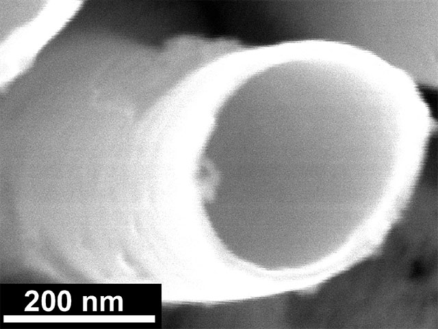
Palladium nanoshell tube (wall thickness about 20 nm)
produced by wetting a porous alumina template
M. Steinhart, U. Gösele et al.,
Adv. Mat. 15, 706 (2003)
Forschung » Nanostrukturierte Template

Nanostrukturierte Template
Zusammenfassung
For the controlled deposition or removal of materials at
predefined locations on a nanometer scale nanostructured
templates or masks play a crucial role. Well-known examples
of masks are those used in microelectronic chip processing
involving typical top-down approaches such as photo- and
electron beam lithography (EBL).
Similarly, focused ion beam (FIB) techniques may be used
to structure masks or materials directly. A top-down
technique presently under development and a potential
major competitor to conventional lithography is nanoimprint
lithography (NIL). The most advanced EBL, FIB, and NIL
equipment combined with deposition and etching systems will
be available for use within the planned CoE, partly in close
collaboration with the companies developing the equipment,
at the nanofabrication facility of technology incubator
(TGZ III) which is presently under construction.
Even though many areas of nanoscience and -technology have
greatly benefited from the availability of top-down lithographic
techniques, in many cases major advances involved nanostructures
fabricated based on self-organized processes. Nanostructures
based on these bottom-up approaches may often be tailored
down to the atomic or molecular level and may cost only a
small fraction of those based on typical lithographical
approaches. Presently, these self-organized structures
have not yet shown the sophistication and complexity which
can be attained by repeated application of lithographic
techniques, but biological structures obviously exemplify
that bottom-up approaches clearly have the ability to
lead to highly complex structures.
Landesgeförderte Projekte
(Förderung 07/2005-06/2008)